IBM Research presented a roadmap for pushing chip patterning beyond 2 nm nodes with High-NA EUV, stochastic-risk reduction, new masks, better resists, and manufacturable process integration.

Overview
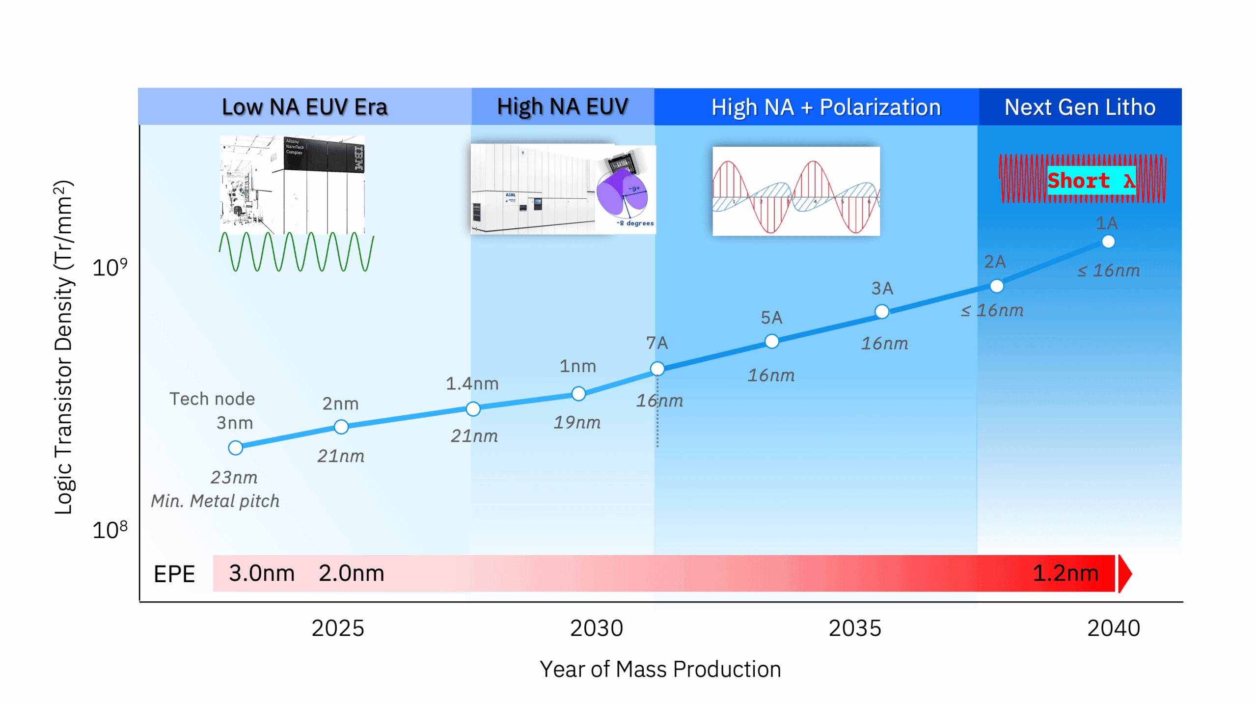
IBM Research used SPIE Advanced Lithography + Patterning 2026 to lay out a connected roadmap for logic patterning below the 2 nm node.
The roadmap brings together High-NA EUV, polarization control, stochastic-risk reduction, next-generation masks, and resist development. The goal is not just smaller features, but manufacturable chips with controlled edge placement error and usable yield.
This sits in the same broader computer-engineering story as 2 nm nanosheet transistor technology, backside power delivery, chiplet packaging, and new design constraints for high-performance AI and mobile hardware.
For software and 3D work, semiconductor scaling still matters because power, memory bandwidth, thermal limits, and accelerator cost shape what kinds of real-time AI, graphics, and robotics systems can actually ship.
Why It Matters
- Connects High-NA EUV research to manufacturable patterning beyond 2 nm nodes.
- Targets edge placement error, stochastic defects, masks, resists, and full process integration.
- Builds on nanosheet transistor scaling and IBM's earlier 2 nm chip work.
- Highlights how physical manufacturing limits shape the future of AI hardware and embedded systems.